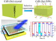
Direct transformation of bulk crystals to single-crystalline crystallographically oriented semiconductor nanowire arrays is presented. Real-time imaging during in situ environmental scanning electron microscopy experiment clearly demonstrates that the nanowire arrays form through a selective vaporization process with respect to the crystallography of wurtzite crystals. Due to the high quality of the prepared semiconductor nanowire arrays, photodetectors constructed from them can present superior optoelectronic performances. Advanced Materials,2016 |